(Hong Kong)

Product Summary
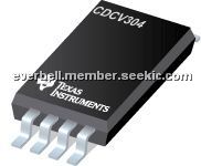
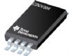
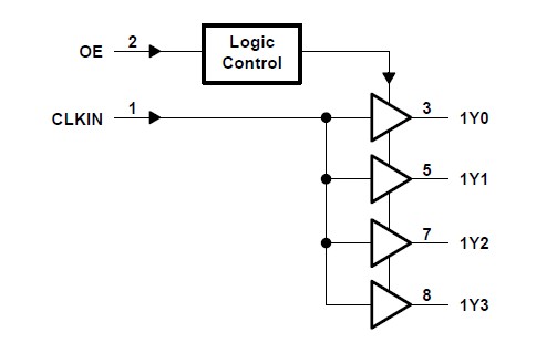
The CDCV304PW is a high-performance, low-skew, general-purpose and PCI-X clock buffer. It distributes one input clock signal (CLKIN) to the output clocks (1Y[0:3]). The CDCV304PW is specifically designed for use with PCI-X applications. The CDCV304 operates at 3.3 V.
Parametrics
CDCV304PW absolute maximum ratings: (1)Supply voltage range, VDD: –0.5 V to 4.3 V; (2)Input voltage range, VI: –0.5 V to VDD + 0.5 V; (3)Output voltage range, VO: –0.5 V to VDD + 0.5 V; (4)Input clamp current, IIK (VI < 0 or VI > VDD): ±50 mA; (5)Output clamp current, IOK (VO < 0 or VO > VDD): ±50 mA; (6)Continuous total output current, IO (VO = 0 to VDD): ±50 mA; (7)Package thermal impedance, θJA: PW package: 230.5℃/W; (8)Storage temperature range, Tstg: –65℃ to 150℃.
Features
CDCV304PW features: (1)General-Purpose and PCI-X 1:4 Clock Buffer; (2)Operating Frequency: 0 MHz to 140 MHz; (3)Low Output Skew: <100 ps; (4)Distributes One Clock Input to One Bank of Four Outputs; (5)Output Enable Control That Drives Outputs Low When OE Is Low; (6)Operates From Single 3.3-V Supply; (7)8-Pin TSSOP Package.
Diagrams
| Image | Part No | Mfg | Description |  |
Pricing (USD) |
Quantity | ||||||||||||
|---|---|---|---|---|---|---|---|---|---|---|---|---|---|---|---|---|---|---|
 |
 CDCV304PW |
Texas Instruments |
Clock Buffer CLOCK BUFFER |
Data Sheet |
|
|
||||||||||||
|
CDCV304PWG4 |
Texas Instruments |
Clock Buffer CLOCK BUFFER |
Data Sheet |
|
|
||||||||||||
|
CDCV304PWRG4 |
Texas Instruments |
Clock Buffer Gen Purpose and PCI-X 1:4 Clock Buff |
Data Sheet |
|
|
||||||||||||
|
CDCV304PWR |
Texas Instruments |
Clock Buffer Gen Purpose and PCI-X 1:4 Clock Buff |
Data Sheet |
|
|
||||||||||||